This project is a redesign of the open source FM synthesiser PreenFM2 created by Xavier Hosxe.
Improvements from the original version:
- fewer and cheaper components
- single PCB (cheaper)
- 4 separate audio channels (on 2 stereo 6.3mm audio jacks)
- stereo DAC chip PCM5102 can be driven directly by the I2S processor's interfaces (faster);
sample resolution can be increased to 24 or 32 bits - headphones stereo amplifier (up to 2 × 175mW on 8ohm loads) on stereo 3.5mm jack
- one extra encoder and separate encoder switches
- all buttons and encoders are handled by a separate STM32F1 processor so they don't need to be constantly scanned
an interrupt (Srf_Int) is generated when a new surface event is detected and the main processor can then interrogate the slave STM32F1 for changed inputs with just a fast SPI transaction - digital volume control (range is -46dBu to 2dBu).
global volume is controller by encoder5 independently by STM32F1 which also converts rotations to a logarithmic scale
STM32F1 can remember previous volume settings and restore them - MIDI interface compliant with 3.3V specifications
- AUX (second) serial interface
- separate analog ground and analog 3.3V supply
The project new schematic
These are the design files for this project (version 1.1):
- Gerber files for PCB manufacture
- PCB mechanical view
- the BOM list
- SMD placement coordinates (for pick and place machines)
- All the OrCAD design files: schematic, layout plus
- the STM32F405 processor CubeMX and its documentation
- STM32F405 test source code
- the STM32F103 processor CubeMX and its documentation
- STM32F103 source code
Below is a simulation of the audio signal path:
| Simulation schematic of the Analog Path to Line Out | |
| Frequency Domain | Time Domain |
and the mixer and headphones amplifier:
| Mixer and Headphones Amplifier Schematic |
| Time Domain |
- The PCM5102 has very good digital filters (with a selection between FIR and IIR with a lower latency).
- R5/C4 is the external recomended low pass filter with a -3dB at 160kHz cutoff.
- PCM5102 output signal is 2.1Vrms ground centred and C3 is decoupling it from the OPA2337 OpAmp which operates at a midpoint of 1.65V (R1,R2 divider).
- R5,R6 are halving the signal so that it stays in the OpAmp swing range.
- R7 is the digital potentiometer (from 120ohm to 10K) and C5 the parasitic capacitance of the pot and R3 protects the OpAmp output in case of a short-circuit.
- The PCM5102 DAC has a dynamic range of 112dB. This translates to a factor of 398107 or about 19 bits of precision. For those extra 3 bits ( over a half word ) the CPU and its
DMA has to transmit 32 bits for each sample and the memory buffers occupy twice as much memory. The most significant half word must be sent first a word swap is needed since the ARM is little endian. - The code explicitly sets the I2S interface as 24 bits transmitted over 32 bits frame. This reduces a little the switching noise over the I2S buses and the DAC full precision of 19 bits fit in the 24 bit of payload.
Bellow are real captures of sine waves at different frequencies. The FFT is computed from the scope trace so the noise floor is much higher than in reality (extra noise is added by the scope's ADC sampling error). The DAC's output capture is taken after the 160kHz filter so the real output voltage is twice what's shown in these captures.
| DAC Output | |||
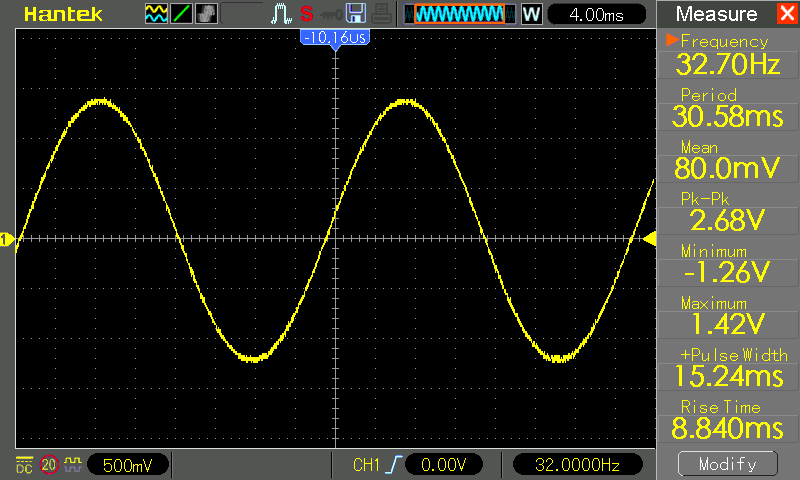 |  | 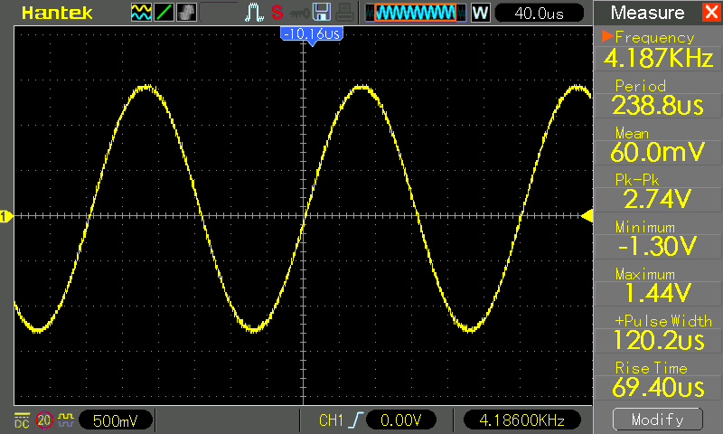 |  |
| Note C1 Sine | Note C6 Sine | Note C8 Sine | FFT at 4.1kHz |
| Line Output | |||
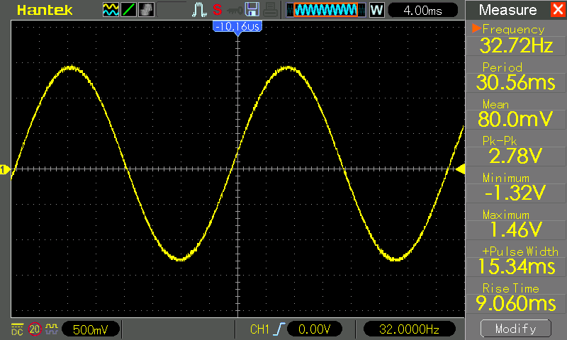 | 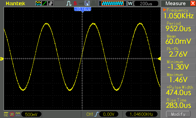 |  | 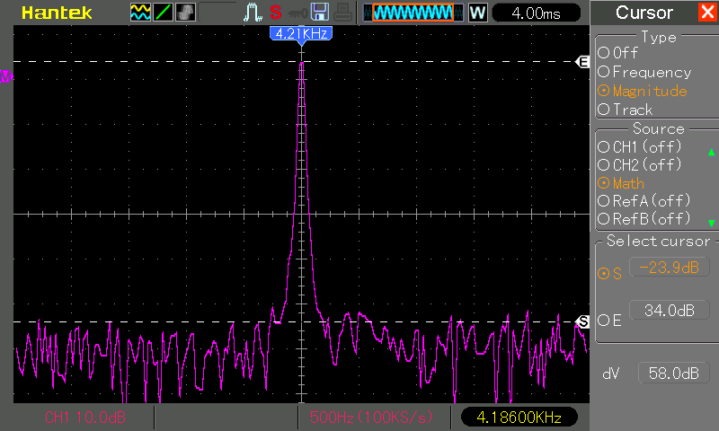 |
| Note C1 Sine | Note C6 Sine | Note C8 Sine | FFT at 4.1Khz |
Even extreme frequencies of 18kHz and 24kHz look very close to sine waves although we only provide the DAC 3 respectively 2 samples per period. This is of course thanks to the FIR filter inside the PCM5102.
The datasheet measures distortions at -1dBFS and some other people reported some performance loss at 0dBFS. The capture bellow still shows a perfect sine wave even for the 6.12V peak-to-peak voltage swing. However I will limit the range in software to -1dBFS ; for 24 bits this equals to (1<<23) * 10^(-1/20) or +/-7476354.
| Extreme Frequency or Amplitude | ||
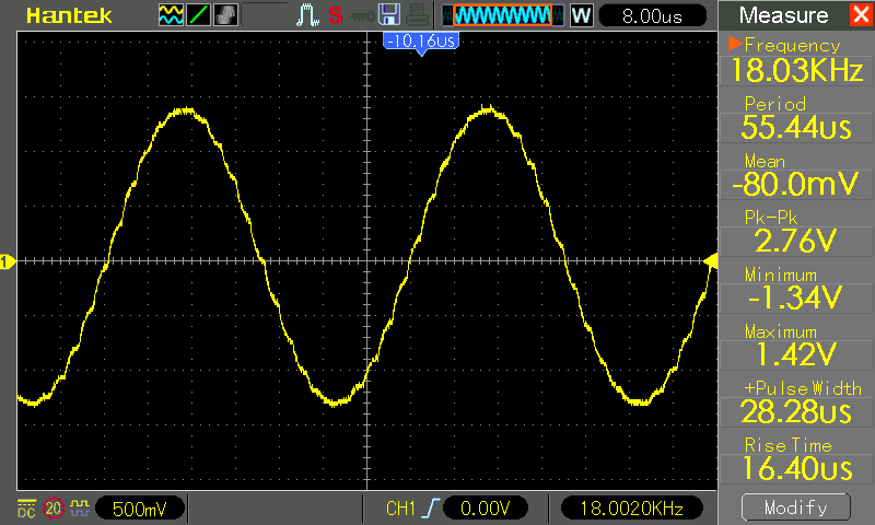 | 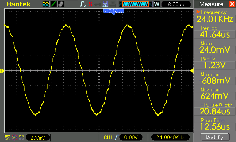 | 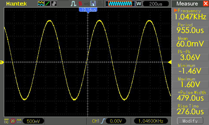 |
| 18kHz DAC out | 24kHz DAC out | 1kHz DAC out 0dbFS |
 |  | |
| 18kHz line out | 24kHz line out | |
- In my initial headphones amplifier design I was using a TDA2822M which has a fixed gain of 39dB (almost 100x) and I was mixing the 4 channles with simple resistor -30dB attenuators while powering the chip from the 5V digital supply. This proved to be a bad ideea since a lot of digital noise was amplified a lot and the sound quality was awful.
- The second iteration of the headphones amplifier will use the LM4880 with only 1.5x voltage gain. The amplifier will provide about 200mW in 8ohms headphones per channel (or 85mW in 32ohms). The 4 channel mixer will use the MC33204 rail-to-rail OpAmp and the headphones amplifier will have its own 5V power supply from a 78L05 regulator.
- This is the schematic for the version which includes a headphone amplifier
- Probably sometimes in the future, when I'll exhaust the current PCBs, I will make a new board.
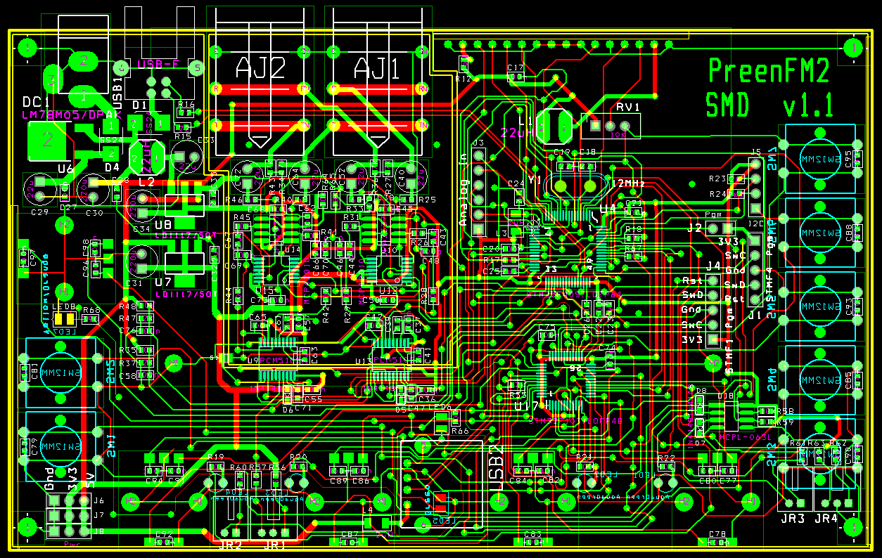
All components have been placed manually and the footprints checked.
The PCB was routed with 10mils traces and 48mils vias, minimum clearance 8mils.
Analog and digital ground planes are not displayed.
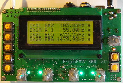 | 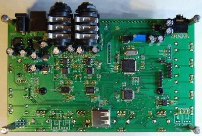 |
| Front Side | Back Side |
Below are links and prices (including shipping) to components I've purchased from Aliexpress (for 10 kits):
So without a case the components price for one PreenFM2 (SMD version) comes to a little more than 30 USD.

If not, do you still have the original PCBs for sale?